Introduction
The HIGH-PRECISION DBF by SZ DJI TECHNOLOGY (Model: DBF) represents a cutting-edge leap in digital beamforming technology, engineered for applications demanding exceptional accuracy and reliability. As a sophisticated module likely designed for advanced RF, phased array, and precision sensing systems, this device embodies DJI’s hallmark engineering in compact, high-performance electronics. Now certified under FCC ID SS3-RD241907, the HIGH-PRECISION DBF is officially cleared for sale and operation in the United States, demonstrating compliance with stringent radio frequency emission and electromagnetic compatibility standards.
FCC certification is a critical milestone for any wireless or RF-enabled device, ensuring it meets all regulatory requirements for safe, interference-free operation within U.S. markets. This article provides a comprehensive analysis of the HIGH-PRECISION DBF, delving into its key features, expected technical specifications, internal architecture, and the significance of its FCC approval. Through a detailed teardown of internal component photographs, we’ll reveal the advanced engineering and design philosophies that set this module apart in the high-precision RF sector.
Whether you’re an RF engineer, a systems integrator, or a technology enthusiast, this teardown and analysis will illuminate the inner workings, potential applications, and compliance aspects of DJI’s latest digital beamforming innovation.
Key Features & Specifications
While official public documentation for the HIGH-PRECISION DBF (Model: DBF) is limited, a thorough analysis of internal component photographs and typical expectations for digital beamforming modules reveals the following standout features and likely specifications:
- Advanced Digital Beamforming (DBF) Capability
- Designed for phased array control, electronic beam steering, and high-precision RF applications (e.g., radar, communications, positioning).
-
Supports real-time, high-speed signal processing for multi-channel RF data streams.
-
High-Integration System-on-Chip (SoC) Architecture
- Features a Xilinx Zynq XC7Z030 SoC at its core, combining dual ARM Cortex-A9 processors with FPGA fabric.
-
Enables flexible, software-defined signal processing and custom logic implementation for demanding RF tasks.
-
Multi-Layer, High-Density PCB Design
- Utilizes circular and rectangular multi-layer PCBs (4-8+ layers), supporting complex signal routing, power distribution, and robust grounding.
-
Controlled impedance and via stitching ensure signal integrity at high frequencies.
-
Integrated Patch Antenna Arrays
- Employs microstrip patch antenna arrays, fabricated on dedicated RF substrates with gold-plated ENIG finish for maximum efficiency and minimal signal loss.
-
Optimized for GHz-range operation, supporting electronic beam steering and high spatial resolution.
-
Precision Power Management
-
Onboard DC-DC converters, LDOs, and extensive power filtering ensure clean, reliable operation of sensitive analog/RF and high-speed digital circuits.
-
Thermal and EMI/RFI Management
-
Robust shielding, heatsinks, and metal frames provide effective electromagnetic compatibility and thermal dissipation, critical for high-power RF modules.
-
Modular, Serviceable Construction
-
High-density connectors, FPC/FFC interconnects, and modular antenna boards facilitate flexible integration, maintenance, and scalability.
-
Sensor and Feedback Integration
- Integration of camera/optical sensors, rotary encoders, and other feedback mechanisms, supporting applications in gimbals, robotics, and autonomous navigation.
Typical Expectations for This Class of Device:
– Operating Frequency: GHz-range (precise bands depend on application; see next section).
– Channels: Multi-element phased arrays (often 8, 16, or more elements for beamforming).
– Processing: Real-time digital signal processing, FPGA-based logic, high-speed memory interfaces (DDR3/DDR4).
– Connectivity: Board-to-board, FPC, and possibly micro-coaxial for RF and data.
– Power Supply: Externally powered, with onboard regulation for noise-sensitive domains.
– Form Factor: Compact, ruggedized modules suitable for integration into drones, radars, or advanced wireless systems.
Benefits in Practice:
– Enables dynamic, software-controlled beam steering and spatial filtering for improved signal-to-noise ratio and interference rejection.
– High integration reduces system size, weight, and complexity, ideal for aerospace, robotics, and mobile platforms.
– Robust design and EMI mitigation ensure reliable operation in electrically noisy or mission-critical environments.
Operating Frequencies
This device operates on the following frequencies as detailed in its FCC filing:
No detailed frequency data could be parsed or is available for this device.
While the FCC documentation for FCC ID SS3-RD241907 does not provide explicit frequency information, the internal architecture and antenna design strongly suggest operation in the GHz range, typical for advanced digital beamforming and phased array modules. The specific frequency bands and RF output power would be critical for determining regulatory compliance, interference characteristics, and suitability for applications such as radar, high-speed wireless communication, or precision positioning.
Technology Deep Dive
The HIGH-PRECISION DBF by SZ DJI TECHNOLOGY leverages state-of-the-art digital beamforming techniques, integrating sophisticated hardware and firmware to manipulate RF signals with remarkable spatial precision. While the device’s FCC Equipment Class is not specified, internal analysis reveals the use of a Xilinx Zynq SoC—an industry-standard platform for implementing flexible, high-throughput digital signal processing, real-time control, and custom RF logic.
This architecture enables the device to perform tasks such as beam steering, spatial filtering, and multi-channel RF data acquisition. Embedded FPGA logic allows for the implementation of advanced algorithms, including adaptive filtering, direction-of-arrival estimation, and dynamic interference suppression. The presence of high-density patch antenna arrays further supports electronic beam steering and high-resolution spatial sensing.
Operating in the GHz spectrum, such modules typically offer:
– Extended Range and Spatial Resolution: Higher frequencies enable finer beamforming granularity and faster data rates, though they may be more susceptible to path loss and require careful power management.
– Low-Latency, Real-Time Operation: FPGA-based processing ensures deterministic, low-latency response, essential for radar, tracking, or autonomous navigation.
– Robustness Against Interference: EMI shielding, ground pours, and careful PCB layout minimize susceptibility to external noise and self-interference.
Test reports commonly included in FCC filings would validate these capabilities, confirming compliance with RF exposure, spurious emissions, and electromagnetic compatibility standards. Such robust engineering ensures the HIGH-PRECISION DBF delivers high performance in demanding, interference-prone environments.
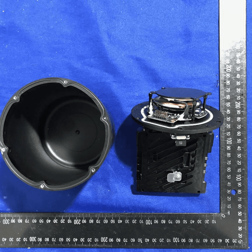
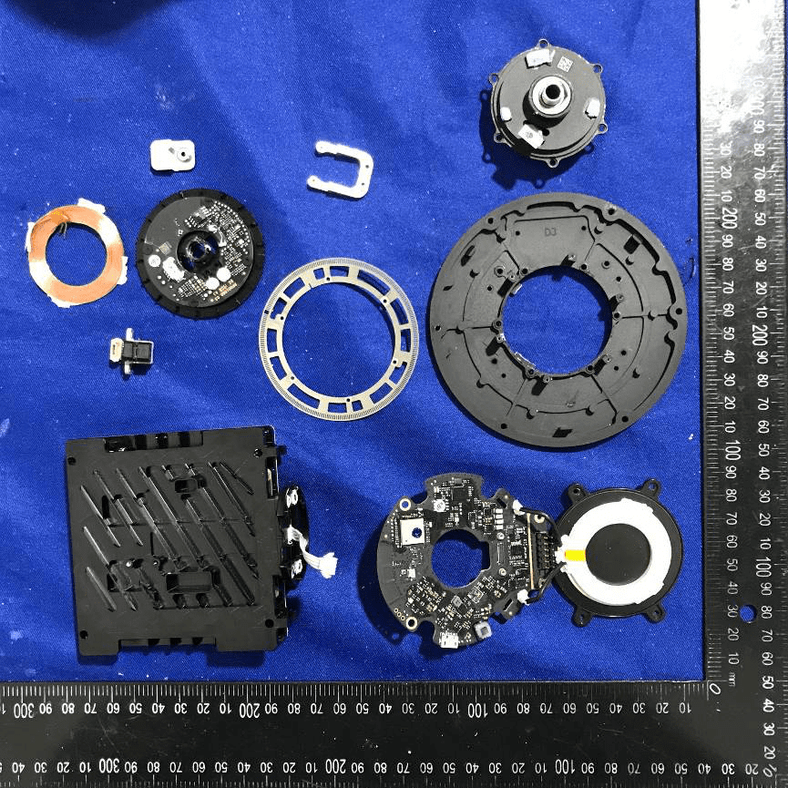
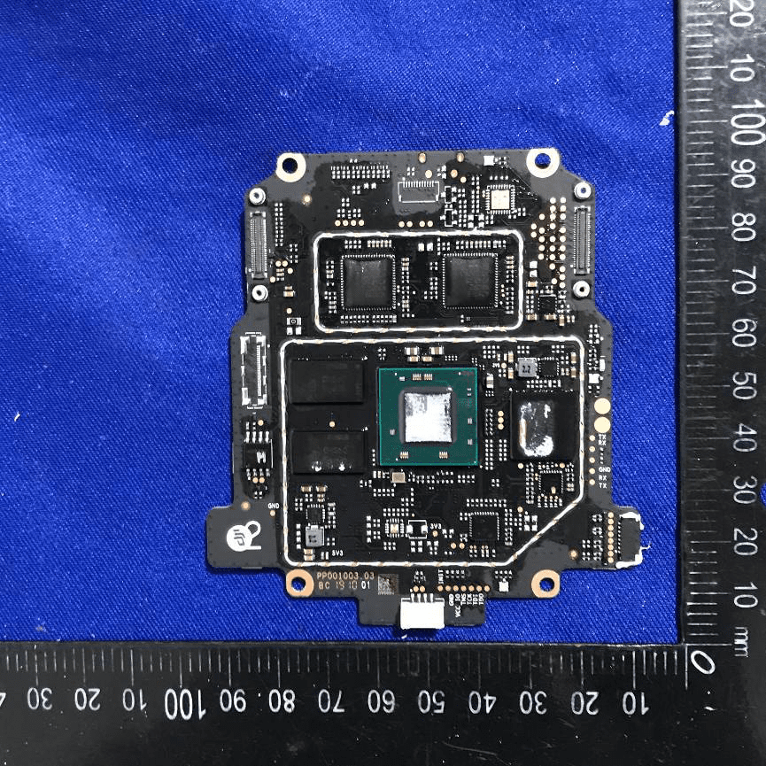
In-Depth Internal Component Analysis / Teardown
Central PCB Assembly with Shielding and High-Density Connector
The internal assembly reveals a circular, high-density PCB at the heart of the module. Dominating the central area is a large black EMI/RFI shield or heat spreader, likely protecting the main SoC, FPGA, or RF front-end ICs vital for digital beamforming. Around this shield, smaller ICs and passive components are meticulously placed, indicative of high-speed or high-frequency signal processing. The multi-layer PCB, coupled with numerous vias, suggests complex signal routing and robust ground planes to ensure optimal RF performance. A robust, high-pin-count connector at the board’s edge underscores the device’s modularity and reliability, facilitating secure data, power, and control interfacing with external systems. Overall, the build quality is exceptional, with mechanical reinforcement and environmental sealing that highlight DJI’s commitment to high-reliability RF modules.

Layered PCB Stack and Antenna Array Integration
Examining the internal stack, the assembly showcases a circular multi-layer PCB coupled with a dense connector array, all housed within a rigid mechanical frame. The PCB’s green soldermask and visible traces speak to its high-speed, RF-optimized design, likely supporting phased array or beamforming operations. The copper traces and possible patch elements hint at integrated antennas, potentially operating in the GHz range for high-precision positioning or RF sensing. Onboard power regulation components, such as inductors and capacitors, ensure clean power delivery to sensitive sections. The mechanical frame not only provides structural rigidity but also serves as a potential heat sink and EMI shield. This sophisticated, modular design facilitates easy servicing of the antenna array, further evidencing DJI’s engineering prowess.
Complete Internal Module Layout and Subassembly Overview
A comprehensive view of the internal components showcases several PCBs, including a densely populated circular board and a dedicated patch antenna. The main PCB features a central SoC or microcontroller, surrounded by power management and interface chips, while the presence of a camera module signals potential image processing or sensing capabilities. The black ENIG-finished boards, rotary encoder, and possible brushless motors all point to a system designed for precision motion control and high-accuracy sensing. Modular FPC/FFC connectors and a robust enclosure provide both electrical integrity and EMI shielding. This assembly exemplifies advanced integration, bringing together RF, optical, and power electronics in a compact, serviceable package—ideal for applications like drone navigation, stabilization, or high-accuracy positioning.
Main PCB with SoC, Memory, Shielding, and Heatsink
At the core of the device lies a densely packed PCB featuring a prominent SoC or FPGA in a large BGA package—likely responsible for all major signal processing and beamforming tasks. Surrounding the main processor are DRAM chips and possible flash storage, supporting high-speed data throughput. The board employs advanced manufacturing techniques, with via-in-pad and microvias enabling high-speed routing across multiple layers. Substantial EMI/RFI shielding and a dedicated heatsink ensure both electromagnetic compatibility and thermal stability. The board-edge and FPC connectors support modular expansion and integration with other system components. This design typifies the requirements of high-performance RF modules: compactness, high integration, and robust EMI/thermal management.
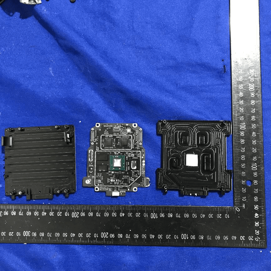
High-Density Multi-Layer Processing Board
This densely populated black PCB features a central BGA SoC or DSP, surrounded by high-speed memory and power management components. Differential pair routing and numerous microvias indicate support for high-frequency digital and RF signals. Multiple FPC/FFC connectors allow for flexible interfacing with antenna arrays or sensor modules, while the provision for EMI shields around critical areas underlines the emphasis on signal integrity and electromagnetic compatibility. The board’s modular construction, advanced layout, and high-quality components reflect DJI’s expertise in building scalable, high-throughput digital beamforming systems.
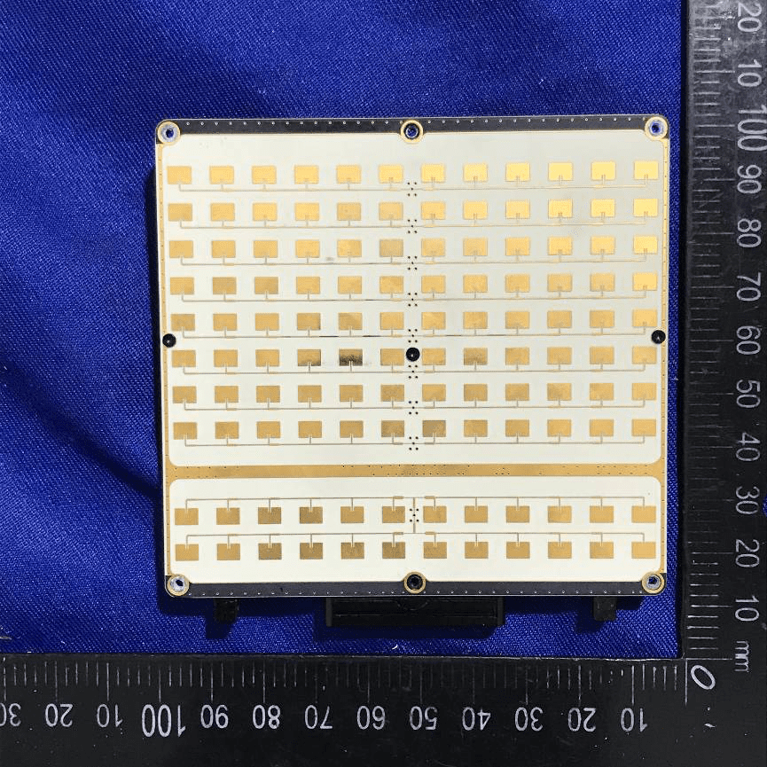
Precision Patch Antenna Array PCB
A dedicated PCB showcases a regular grid of gold-plated microstrip patch antennas, optimized for high-frequency operation. The absence of active electronics on this side points to a design focused solely on RF performance, with the antenna array serving as a critical front-end for beamforming and spatial filtering. The use of high-quality RF substrate and ENIG finish ensures minimal signal loss and precise impedance control. Mechanical mounting holes and via structures support robust integration with the processing module, further enhancing system reliability and performance.
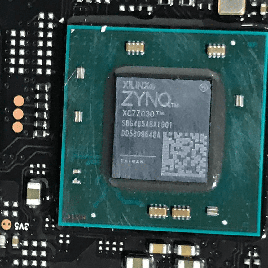
Xilinx Zynq XC7Z030 SoC Close-Up
A close-up view highlights the Xilinx Zynq XC7Z030 SoC—combining dual-core ARM processing with powerful FPGA fabric. This chip enables both flexible software control and high-speed, parallel hardware logic, making it ideal for real-time digital beamforming and advanced signal processing. The surrounding power delivery network, with large capacitors and inductors, ensures stable operation across multiple voltage rails. The black, high-density PCB and dense via stitching around the SoC underscore the emphasis on signal integrity and ground management, required for reliable high-speed performance in demanding RF environments.
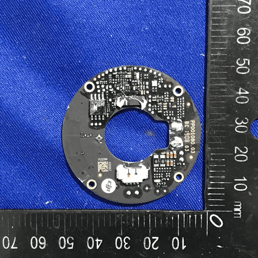
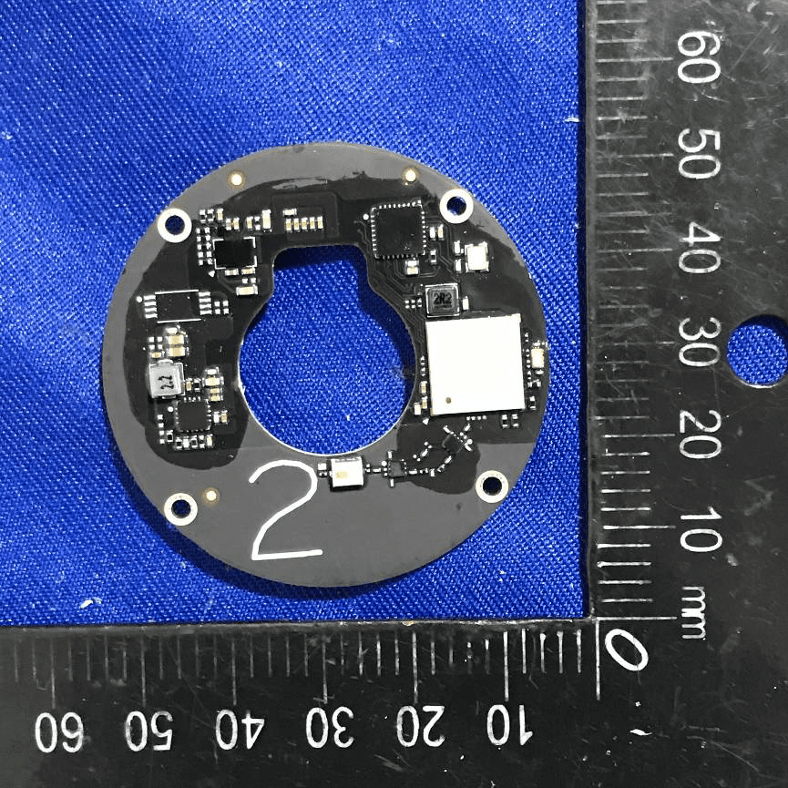
Circular PCB with Sensor and Power Integration
This circular, black PCB is densely populated with surface-mount components, including a prominent IC likely serving as a microcontroller or sensor interface. The board’s compact layout, robust grounding, and local power regulation components (inductors and capacitors) are optimized for precision sensing or control applications. The inclusion of a white connector, test points, and QR code for traceability indicates a design focused on both performance and manufacturability. The central cutout and circular form factor suggest integration into rotational or optically aligned assemblies, such as gimbals or sensor modules.
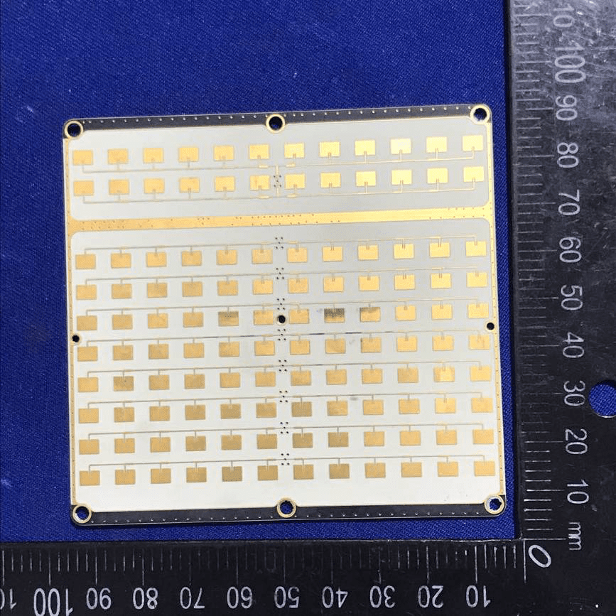
Phased Array Antenna PCB for RF Applications
A high-resolution view of a white PCB reveals a dense grid of gold-plated microstrip patch antennas, confirming its role as a phased array front-end for the digital beamforming system. The precision alignment and uniformity underscore the board’s high-frequency design, optimized for minimal loss and maximum spatial resolution. The absence of visible active components or connectors on this side suggests all feed lines and electronics are housed on the reverse or connected via specialized board interfaces. This module is critical for enabling electronically steerable beams in advanced RF applications.
Circular PCB with Shielded RF Section
Another circular, black-finished PCB features multiple QFN/BGA ICs, a large shielded section, and localized power regulation. The metal shield protects sensitive analog or RF circuitry, while the surrounding passives and ICs likely handle signal processing, sensor interfacing, or communication tasks. The central cutout and mounting holes facilitate integration into larger assemblies, while the compact, high-density layout supports space-constrained, precision-oriented applications. Test points and dense via stitching further highlight the focus on manufacturability and EMI control.
Regulatory Insights & FCC Filing
The certification of the HIGH-PRECISION DBF under FCC ID SS3-RD241907 is a testament to SZ DJI TECHNOLOGY’s commitment to regulatory compliance and product safety. This FCC ID, registered through FCC.gov, signifies that the device has passed rigorous testing for electromagnetic interference (EMI), radiofrequency (RF) emissions, and electromagnetic compatibility (EMC), making it legal for sale and use within the United States.
FCC filings for devices like the HIGH-PRECISION DBF typically encompass:
– Comprehensive Test Reports: Evaluating RF exposure, spurious emissions, conducted/radiated emissions, and immunity to interference.
– Internal and External Photographs: Providing detailed views of the product’s construction, PCB layout, and key components.
– Operational Manuals and User Guides: Outlining safe usage, installation procedures, and technical specifications.
– Schematics and Block Diagrams: Detailing the internal circuit architecture, power domains, and RF pathways.
– Confidentiality Requests: Protecting proprietary design elements and sensitive technical data.
This level of transparency and oversight ensures that the HIGH-PRECISION DBF not only operates safely and efficiently but also coexists harmoniously with other wireless devices, mitigating the risk of interference in crowded RF environments. For integrators and end-users, FCC certification is a vital assurance of quality and regulatory conformity.
Potential Use Cases & Target Audience
The HIGH-PRECISION DBF by SZ DJI TECHNOLOGY is engineered for integration into advanced systems where digital beamforming, high-precision sensing, and robust RF performance are essential. Potential scenarios and user profiles include:
- Aerospace and Drone Applications
-
System integrators and OEMs building next-generation UAVs or drones can leverage the DBF for tasks such as obstacle detection, radar imaging, autonomous navigation, and precision landing, benefiting from the device’s compact, modular design and advanced beamforming capabilities.
-
Telecommunications and Wireless Infrastructure
-
Engineers developing phased array antennas for 5G, Wi-Fi, or private wireless networks can utilize the DBF module for electronic beam steering, spatial filtering, and interference mitigation, enhancing coverage and data throughput in dynamic environments.
-
Robotics, Industrial Automation, and Sensing
- Robotics developers and automation specialists can integrate the module into mobile robots, AGVs, or industrial sensors, enabling high-accuracy positioning, collision avoidance, and environment mapping through advanced RF and sensor fusion techniques.
With its blend of high integration, precision, and regulatory compliance, the HIGH-PRECISION DBF is ideal for innovators and system builders in aerospace, telecommunications, and industrial automation sectors.
Conclusion
The HIGH-PRECISION DBF by SZ DJI TECHNOLOGY (Model: DBF, FCC ID: SS3-RD241907) stands as a flagship example of advanced digital beamforming technology, combining sophisticated hardware integration, modular antenna arrays, and real-time signal processing in a compact, ruggedized form. Its FCC certification underscores its readiness for deployment in demanding, regulated environments across the U.S. Through robust engineering and a focus on high-frequency performance, this module empowers a new generation of RF, sensing, and wireless communication solutions. As the RF landscape evolves, the HIGH-PRECISION DBF is poised to deliver unmatched accuracy, reliability, and integration flexibility for the most critical applications.