Introduction
The DATALINK PRO by SZ DJI TECHNOLOGY stands as a robust wireless communication module engineered for demanding, high-reliability data transmission. As part of DJI’s professional ecosystem, this device is tailored for applications where secure, high-speed wireless links are essential—think UAV telemetry, industrial remote control, or mission-critical robotic operations. With its advanced internal architecture and focus on RF integrity, the DATALINK PRO is designed to deliver low-latency, interference-resistant data connections, even in challenging environments.
A notable highlight is its FCC certification under FCC ID SS3-ZT300G1604. While there is no published grant date, registration with the FCC signifies that the DATALINK PRO meets strict US standards for radio frequency (RF) emissions and electromagnetic compatibility (EMC). This compliance is a prerequisite for legal sale and operation within the United States, assuring users that the device will not cause harmful interference and is safe for integration into professional systems.
This article delivers a comprehensive analysis of the DATALINK PRO, delving into its key features, wireless operating specs, internal hardware design, and regulatory insights. Whether you are an RF engineer, system integrator, or tech enthusiast, read on for a deep dive into what makes this wireless module a standout in its class.
Key Features & Specifications
Detailed public specifications for the DATALINK PRO (Model: PRO) are limited, but based on FCC documentation and teardown analysis, several key features and performance expectations can be outlined:
- High-Reliability Wireless Data Link
- Engineered for professional, industrial, and UAV applications requiring robust, low-latency wireless communication.
- Typical use cases include drone telemetry, industrial automation, and remote robotics.
- FCC Certified (FCC ID SS3-ZT300G1604)
- Compliant with stringent US RF emission standards, ensuring legal operation and minimal interference with other devices.
- Operating Frequency
- Utilizes the 903–925.5 MHz spectrum, an ISM band known for long-range, non-line-of-sight wireless communication.
- Output power is carefully regulated for optimal range and compliance.
- RF Performance and Signal Integrity
- Premium PCB design (e.g., black ENIG finish, gold-plated traces) for superior signal integrity and EMI control.
- Robust ground pours, stitching vias, and controlled impedance traces for reliable high-frequency operation.
- Antenna Flexibility
- Support for external high-gain antennas via gold-plated SMA connectors, maximizing adaptability for different environments.
- Professional-Grade Construction
- Metal enclosures and internal shielding for outstanding electromagnetic compatibility (EMC) and mechanical durability.
- Modular PCB architecture for easy integration and serviceability.
- Interfaces
- Micro-USB for configuration, updates, or power (depending on deployment).
- FPC/FFC connectors and test points for manufacturing, debugging, and field service.
- Power Management
- Multiple regulated power domains (analog, digital, RF) for stability and low-noise operation.
- On-board voltage regulation and filtering components to ensure clean supply rails.
- Typical Expectations for This Category
- Devices in this class generally offer:
- Data rates suitable for telemetry and control (hundreds of kbps to several Mbps).
- Range extending to several kilometers, depending on antenna and environment.
- Secure communication protocols and robust error correction.
While some specifics (e.g., exact data rates, supported protocols) are not publicly available, the DATALINK PRO’s construction and certification signal a product designed for high-stakes, interference-prone environments where reliability is paramount.
Operating Frequencies
The DATALINK PRO operates within the following frequency range and power parameters as detailed in its FCC filing:
| Frequency Range (GHz) | Output Power (mW) | FCC Rule Part |
|---|---|---|
| 903-925.5 333 mw15c1 | 333 | 15C1 |
Key Considerations:
– 903–925.5 MHz Band: This ISM band is favored for long-range, robust wireless links, particularly in applications where penetration through obstacles and minimal interference are critical.
– Output Power: The specified power level is optimized for regulatory compliance while enabling reliable operation over extended distances.
– FCC Rule Part 15C1: Indicates unlicensed, but tightly regulated, operation under Part 15 of FCC rules—common for industrial, scientific, and medical wireless devices.
Understanding these parameters is vital for system integrators and RF engineers assessing the DATALINK PRO’s suitability for their application, as they define the device’s legal use, achievable range, and potential for co-existence with other wireless systems.
Technology Deep Dive
The DATALINK PRO’s primary technology focus is high-reliability, license-free RF data communication. Operating in the sub-GHz ISM band (903–925.5 MHz), the module leverages proven wireless technologies tailored for robust, interference-resistant links. This frequency range is less congested than 2.4 GHz, offering better penetration through obstacles and reduced risk of cross-talk from consumer Wi-Fi or Bluetooth devices.
While the equipment class is not explicitly listed, the hardware analysis reveals a design that prioritizes:
– Controlled Impedance RF Routing: Ensures minimal signal loss and reflection, critical for high data integrity over wireless links.
– External Antenna Support: SMA connectors allow the use of high-gain or specialized antennas, extending range and flexibility.
– Multi-Layer PCB Architecture: Separates analog, digital, and RF domains, reducing noise and cross-interference.
These design choices support long-range, low-latency communication, ideal for telemetry in UAVs, industrial remote controls, and secure wireless networking. The power levels and frequency band strike a balance between range, regulatory compliance, and power consumption. Internal test points and modular connectors indicate a device built with both performance and maintainability in mind.
In-Depth Internal Component Analysis / Teardown
Internal View: PCB and Molded Antenna Structure
The internal architecture reveals a meticulously engineered black PCB, featuring wide gold traces and a distinct molded plastic antenna structure. At the heart of the board sits a prominent QFN or LGA package IC, which, based on its placement near the antenna, is likely responsible for RF transceiver or microcontroller duties. Surrounding this are several smaller passive components and what appears to be a voltage regulator, ensuring stable power delivery to sensitive RF sections. The PCB layout is optimized for RF performance, with extensive ground pours and stitching vias to maintain signal integrity and minimize electromagnetic interference. The molded antenna, connected through a carefully designed feedline, suggests operation in ISM bands, and the compact, integrated design reflects the high standards expected in modern UAV and telemetry modules. Overall, the build quality is excellent, emphasizing reliability and RF efficiency.

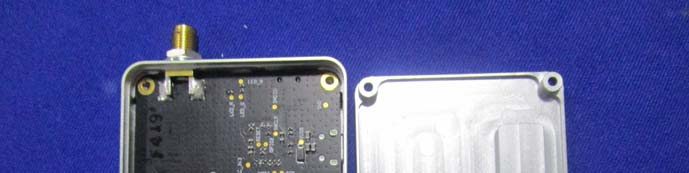
Disassembled PCB with Metallic Enclosure
A deeper look at the device reveals a section of the PCB housed within a precision-machined metallic enclosure, acting as both structural support and EMI shield. A major QFP or QFN IC is centrally located, likely orchestrating core communication or control functions. The PCB’s gold-plated pads and high-density component arrangement point to a multi-layer design, with wide traces specifically routed for RF signals leading to a gold SMA connector. This configuration enables connection to high-performance external antennas, vital for extended range and reliability. The presence of a micro-USB interface suggests ease of configuration or firmware updates. A crystal oscillator nearby provides precise timing, critical for stable RF communication. The overall design underscores a commitment to robust RF performance, modularity, and professional-grade construction.

PCB section with RF routing and SMA connector in metal enclosure.
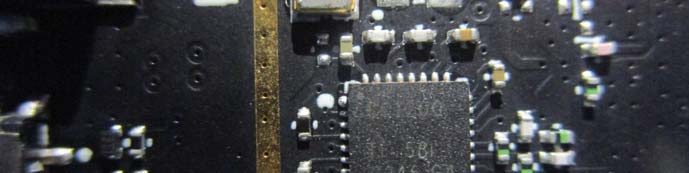
PCB Segment with Shield and Power Domains
This internal view highlights a densely populated area of the PCB surrounded by a metallized shield, emphasizing EMI protection for sensitive circuits. Multiple ICs in SOIC and QFN packages are visible, with one labeled ‘HG3101’—likely a specialized RF or power management component. The board is clearly multi-layered, with numerous test points and labeled power domains (e.g., VCC_RF), enabling precise separation of analog, digital, and RF circuits. The FPC/FFC connector hints at modular expansion or interfacing with auxiliary boards. The shield itself is engineered for optimal grounding contact, minimizing radiated emissions. These features collectively demonstrate sophisticated power management, modular integration, and a strong focus on maintaining RF integrity in high-frequency environments.

High-density PCB under EMI shield with labeled power domains.
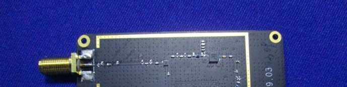
RF Section with SMA Connector and Metal Enclosure
A segment of the PCB dedicated to RF circuitry is revealed with the metal enclosure removed. The area is relatively sparse, featuring several SMD passives and test points, indicative of a section optimized for RF filtering or antenna matching rather than digital processing. The gold SMA connector enables external antenna attachment, a design choice favoring flexibility and enhanced range. Grounding is reinforced through multiple mounting holes and ground pours, leveraging the metal enclosure for superior EMI shielding. The overall construction is robust, with a clear emphasis on mechanical durability and high-frequency signal integrity—hallmarks of a professional-grade RF data link device.
RF section with SMA connector and robust metal EMI shielding.
Close-Up: Major IC and Gold Trace
This close-up provides a detailed look at a key IC—possibly a microcontroller or RF transceiver—situated adjacent to a prominent gold trace, likely serving as an RF signal path or ground pour. The black ENIG-finished PCB and multi-layer design are evident, supporting both RF and power integrity. A small crystal oscillator is positioned nearby, ensuring precise timing for high-frequency operations. Numerous vias and test points enhance testability and signal grounding. The careful layout and use of premium materials reflect a focus on minimizing EMI and maximizing wireless performance, essential for reliable, high-speed data transmission.
Close-up of main IC with RF trace and crystal oscillator.
RF Front-End and Antenna Interface
A clear view of the RF front-end shows a black PCB with gold-plated edge connectors and a solid ground pour. A small IC, likely a low-power amplifier or RF switch, manages the signal path to the adjacent SMA connector, which facilitates external antenna integration. The design employs controlled impedance traces and thorough ground stitching, ensuring optimal RF performance and minimal loss. Sparse component placement further reduces noise and interference, underscoring the module’s commitment to high-fidelity wireless communication in professional settings.
RF front-end with SMA antenna connector and gold ground pour.
RF Shielding and Component Layout
This close-up reveals a section of the PCB characterized by a gold-plated border with dense via stitching, forming an effective RF shield ground ring. A centrally placed IC, surrounded by carefully arranged passives, is likely part of the RF transceiver or power management subsystem. The compact, multi-layer design and premium finish highlight the device’s professional pedigree. While no connectors or antennas are immediately visible, the layout is consistent with high-frequency, low-noise design best practices, crucial for maintaining signal integrity in demanding RF environments.
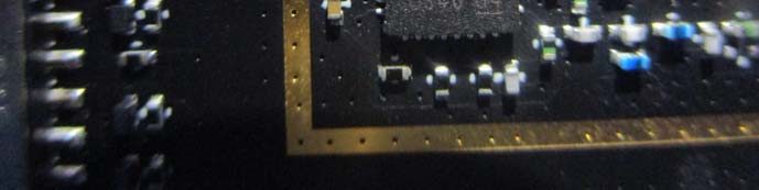
PCB close-up with RF shield ground ring and central IC.
Regulatory Insights & FCC Filing
The DATALINK PRO, registered under FCC ID SS3-ZT300G1604, demonstrates full compliance with US regulatory requirements for RF emissions and electromagnetic compatibility. Although a formal grant date is not listed, its FCC registration ensures it has been rigorously evaluated for safe and interference-free operation in the United States. This certification is critical, as it legally authorizes the device for commercial sale and deployment in professional environments.
Typical FCC filings for devices like the DATALINK PRO include comprehensive documentation:
– RF Exposure Reports: Verifies that the device’s emissions are within safe limits for human exposure.
– EMC Test Results: Ensures the device does not cause or suffer from undue electromagnetic interference.
– Internal and External Photographs: Provide visual confirmation of construction and labeling.
– User Manuals and Operational Descriptions: Outline safe and compliant usage.
– Schematics and Block Diagrams: Detail circuit design and component interconnections.
For engineers, integrators, and regulatory specialists, the FCC ID SS3-ZT300G1604 serves as a guarantee of both technical quality and legal compliance, streamlining system integration and reducing certification overhead in broader deployments.
Potential Use Cases & Target Audience
With its robust design and FCC-certified wireless performance, the DATALINK PRO by SZ DJI TECHNOLOGY is suited for a range of demanding professional scenarios:
- Commercial UAV and Robotics Integrators
- Ideal for drone telemetry, real-time video downlink, or command-and-control applications where reliable, long-range communication is mission-critical.
- Industrial Automation and Remote Monitoring
- Enables secure wireless links in environments with high EMI, such as factories or remote infrastructure, supporting SCADA systems, sensor networks, or machine-to-machine communication.
- Professional System Developers and OEMs
- Provides a ready-to-integrate, regulatory-cleared RF module for custom wireless systems, reducing time-to-market and compliance risk for new products.
Even in the absence of a specifically defined end-user profile, the DATALINK PRO’s feature set and construction clearly target technical professionals seeking high-reliability, high-performance RF data links.
Conclusion
The DATALINK PRO by SZ DJI TECHNOLOGY (Model: PRO, FCC ID SS3-ZT300G1604) exemplifies the cutting edge in professional-grade wireless communication modules. Its advanced RF design, premium internal construction, and robust regulatory compliance make it a compelling choice for applications where reliability, range, and signal integrity are non-negotiable. With its FCC certification, users can be confident in both performance and legal compliance, positioning the DATALINK PRO as a key enabler for next-generation UAV, industrial, and remote monitoring solutions. As wireless demands continue to grow, the DATALINK PRO sets a high bar for secure, high-performance RF data links in the professional market.