Introduction
SZ DJI TECHNOLOGY, a prominent name in the world of advanced technology, has once again captured attention with its latest device, as documented in the FCC.gov filing under FCC ID SS3-201309002. While the exact model name remains unspecified, this device is undoubtedly a testament to DJI’s commitment to innovation and quality. The Federal Communications Commission (FCC) certification, though not yet granted, is a crucial step in ensuring that the device meets the stringent radio frequency (RF) emission standards required for legal sale and operation in the United States. This blog post aims to provide an in-depth analysis of the device’s key specifications, technology, and internal components, offering valuable insights into its regulatory compliance and potential use cases.
Key Features & Specifications
While the official detailed specifications for the SZ DJI TECHNOLOGY device are sparse, we can make some educated expectations based on its FCC filing and typical characteristics of similar devices:
- Wireless Communication: Likely supports 2.4 GHz frequency operations, potentially for Wi-Fi or Bluetooth connectivity.
- Compact Design: The device’s design emphasizes compactness, suggesting it is part of a larger system or module.
- Robust Build Quality: Emphasis on maintaining signal integrity and minimizing interference through RF shielding and antenna design.
- Power Regulation: The presence of capacitors and inductors indicates a focus on RF stability and power management.
These features suggest a device designed for effective wireless communication, with a focus on integration into larger systems. The lack of explicit details in the FCC filing highlights the importance of analyzing internal components to infer its capabilities.
Technology Deep Dive
The SZ DJI TECHNOLOGY device operates in the 2.4 GHz frequency band, a common range for Wi-Fi and Bluetooth communications. This frequency band is known for its balance between range and data throughput, making it ideal for consumer electronics that require reliable wireless connections. The use of 2.4 GHz also implies potential susceptibility to interference from other devices operating in the same range, necessitating robust design and shielding to maintain performance.
The implications for performance include moderate power consumption, suitable for battery-powered applications, and a typical range of up to 100 meters, depending on environmental conditions. The choice of frequency suggests a focus on widespread compatibility and ease of integration into existing wireless ecosystems.
In-Depth Internal Component Analysis / Teardown
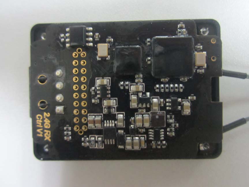
The first internal image reveals a densely populated PCB, painted in black, likely constructed from FR4 material. The board’s compact layout features several integrated circuits (ICs), though specific part numbers are not visible. The ‘2.4G RX’ marking suggests these ICs are crucial for RF communication, possibly for Wi-Fi or Bluetooth. Two protruding wires serve as antennas, enhancing its wireless capabilities. The presence of metal shields indicates effective EMI/RFI protection, crucial for maintaining signal integrity. Overall, this board appears to be a core component of a wireless communication system, expertly designed for RF stability and compact integration.
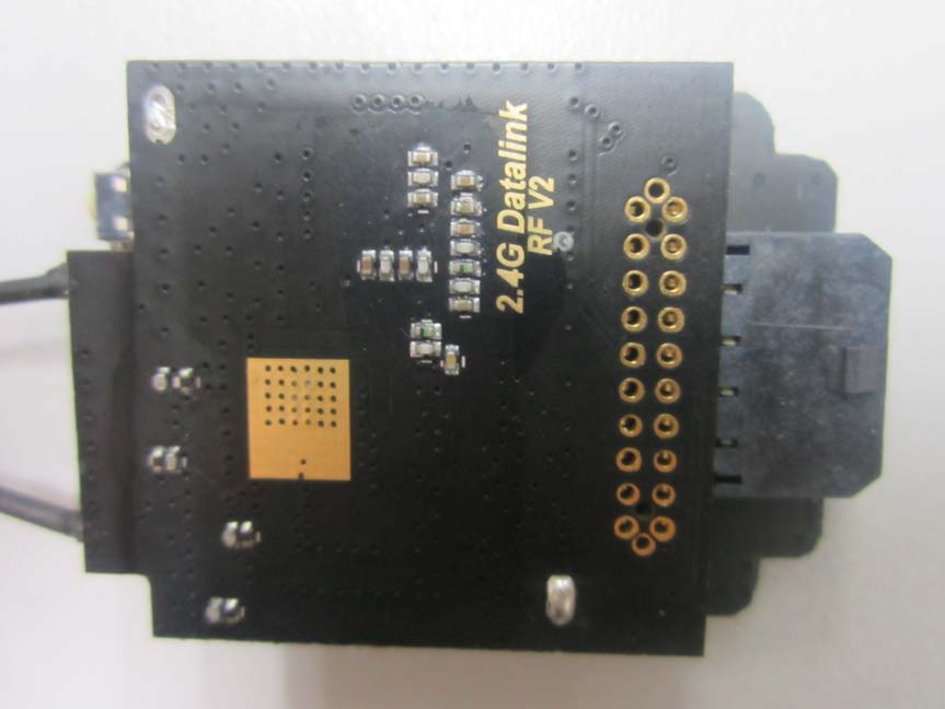
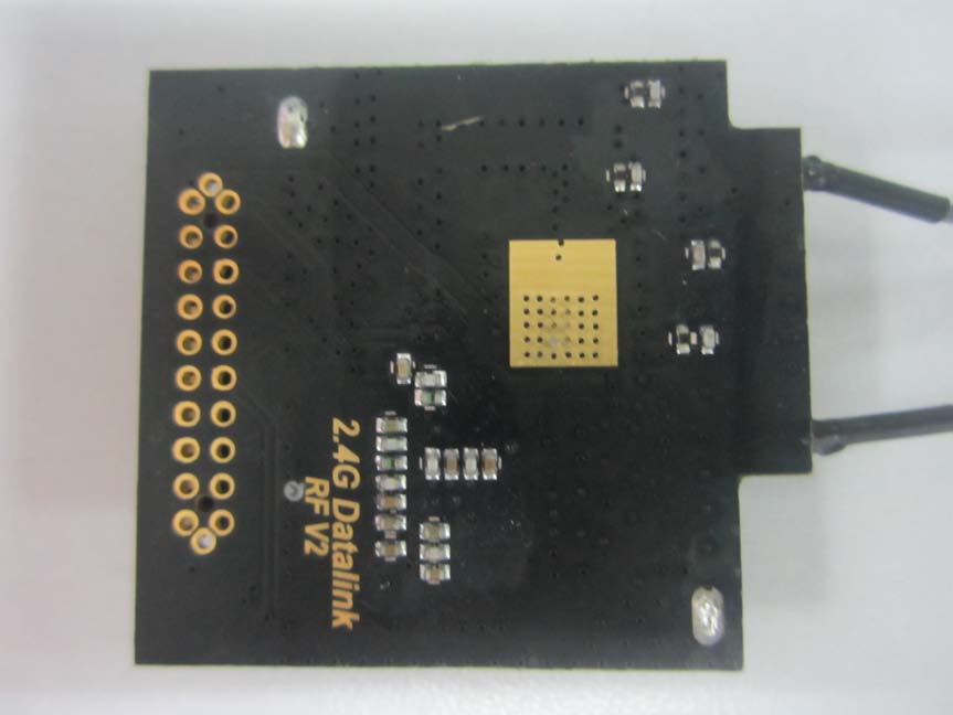
The next image showcases the underside of the PCB, where a large connector is prominently featured. This connector likely facilitates interfacing with other components or systems, possibly for data or power transmission. While no explicit shielding is visible, the design hints at a focus on modularity and integration. The text ‘2.4G Datalink RF V2’ reinforces the device’s emphasis on RF communication, likely in the 2.4 GHz band. This side of the PCB, though less populated, is integral to the device’s connectivity and modular design.
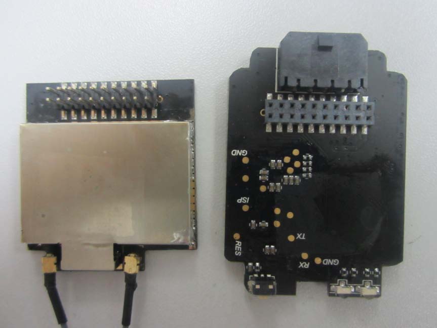
This image presents a dual-PCB configuration, with coaxial connectors suggesting external antenna use. The left PCB, partially obscured by a metal shield, likely houses critical RF components, ensuring robust EMI/RFI protection. The right PCB features a multi-pin connector, indicative of interfacing capabilities with other modules. The design emphasizes modularity and RF performance, with a clear focus on maintaining signal integrity across both boards.
The central IC in this image, although partially obscured, is likely a microcontroller or SoC, responsible for core processing tasks. The crystal oscillator nearby provides essential timing signals. Two coaxial connectors suggest the use of external antennas, enhancing the device’s RF communication capabilities. The layout, with a clear distinction between analog and digital components, indicates a well-thought-out design for minimizing interference and optimizing signal integrity.
This sparse PCB features wire antennas, likely for 2.4 GHz communication, and several through-hole pads, hinting at potential interfaces for power or data connections. The straightforward design suggests a focus on cost-effectiveness and basic functionality, making it ideal for integration into larger systems as a transceiver module.
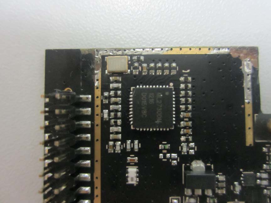
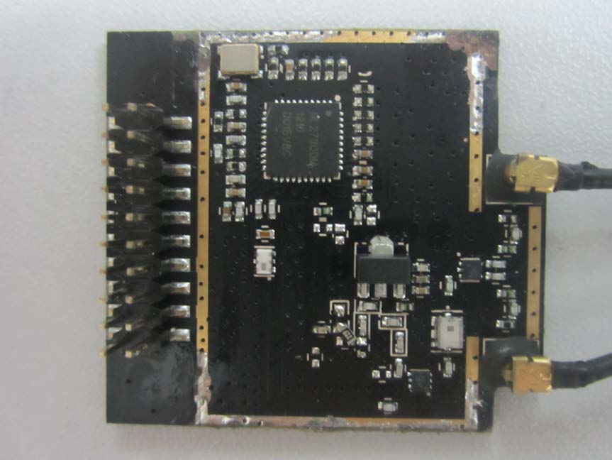
The prominent IC in this image, marked ‘IC 73004’, is likely a microcontroller or application-specific IC. The QFP package is common for such components, indicating its role in processing or control functions. The nearby crystal oscillator ensures precise timing, while the visible power components suggest robust power management. This section of the board, with its straightforward design, highlights the device’s focus on providing essential interfaces and control capabilities.
Regulatory Insights & FCC Filing
The FCC ID SS3-201309002 signifies that the SZ DJI TECHNOLOGY device complies with US electromagnetic interference standards, a crucial requirement for its legal sale and operation. Although the grant date is not yet specified, registration with the FCC ensures that the device has undergone rigorous testing for RF exposure, electromagnetic compatibility (EMC), and other regulatory requirements. FCC filings typically include test reports, internal and external photos, user manuals, and schematics, providing comprehensive insights into the device’s compliance and capabilities.
Potential Use Cases & Target Audience
Given its features and technology, the SZ DJI TECHNOLOGY device is ideal for several practical applications:
- Consumer Electronics: As a wireless communication module, it can be integrated into smart home devices, enhancing connectivity and control.
- Industrial Automation: Its robust RF performance makes it suitable for industrial IoT applications, where reliable wireless communication is critical.
- Drones and Robotics: The device’s compact design and RF capabilities make it a perfect fit for drones and robotic systems, requiring efficient and reliable remote control.
Conclusion
The SZ DJI TECHNOLOGY device, under FCC ID SS3-201309002, represents a significant step in wireless communication technology. Its FCC certification underscores its compliance with stringent RF standards, affirming its readiness for the US market. Through detailed analysis of its internal components and technology, we gain insights into its design philosophy and potential applications. As a versatile and robust module, it holds promise for various industries, reinforcing DJI’s position at the forefront of technological innovation.