Introduction
The DATALINK PRO from SZ DJI TECHNOLOGY stands at the forefront of wireless communication modules engineered for demanding telemetry and data transmission scenarios. While detailed consumer-facing documentation is limited, the device’s robust internal design and regulatory filings reveal a highly capable wireless link solution, likely intended for integration into professional-grade UAVs, industrial systems, or ground stations. The DATALINK PRO, model PRO, is certified under FCC ID SS3-ZT300A1604—a mark of compliance with stringent US regulations for radio frequency (RF) emissions and electromagnetic compatibility.
Although the device has no listed grant date, its inclusion in the FCC database confirms it meets all legal and technical prerequisites for sale and operation within the United States. This article provides a comprehensive, expert-driven analysis of the DATALINK PRO, covering its key features, wireless specifications, operating frequencies, internal hardware, and the significance of its regulatory status. Through teardown insights and technical breakdowns, we’ll uncover why this module exemplifies cutting-edge design and reliability in wireless data communications.
Key Features & Specifications
While official public documentation for the DATALINK PRO is sparse, in-depth analysis of its internal construction and FCC filings allows us to infer several high-level features and specifications typical of advanced wireless telemetry modules:
- High-Performance Wireless Data Link
-
Designed for robust, long-range, low-latency wireless communication, suitable for professional UAVs or industrial telemetry.
-
Advanced RF Design
- Multi-layer PCB (likely 4+ layers) with controlled impedance routing and extensive ground stitching, ensuring signal integrity and minimizing electromagnetic interference.
-
EMI/RFI shielding via metallic cans and enclosure design, critical for reliable operation in RF-dense environments.
-
High-Quality Components
-
Surface mount assembly with premium components, including:
- Texas Instruments CC1200 RF transceiver (sub-1 GHz operation)
- Multiple microcontrollers or SoCs (for protocol handling, data processing)
- Local power regulation (switching regulators, LDOs, high-quality capacitors/inductors)
- Precision crystals/oscillators for accurate RF timing
-
Flexible Connectivity
-
Likely supports a variety of interfaces, including micro-USB (for data, power, or firmware update), gold-plated edge connectors, and RF connectors (U.FL, MMCX, or similar) for external antennas.
-
Compact, Modular Construction
- Dense, space-efficient PCB layout with modular, shielded sections for ease of serviceability and integration.
-
Test points and debug headers for manufacturing and field diagnostics.
-
Operating Frequency Versatility
- Primary operation in sub-1 GHz ISM bands (notably 903–925.5 MHz), ideal for long-range, interference-resistant data links.
- Output power and frequency range tailored for maximum range while adhering to regulatory limits.
Benefits & Practical Implications:
– Reliability: EMI shielding and robust power filtering ensure stable performance even in noisy RF environments.
– Range & Penetration: Sub-1 GHz operation allows for superior range and penetration compared to higher-frequency links, making it suitable for challenging terrains or urban use.
– Serviceability: Modular design with removable shields and accessible test points facilitates maintenance and troubleshooting.
– Integration: Compact footprint and flexible interfaces allow easy integration into larger UAV systems or ground stations.
While precise consumer-facing specifications (such as data rate, latency, or supported protocols) are not publicly disclosed, the engineering choices evident in the teardown strongly indicate a device engineered for demanding, mission-critical wireless data applications.
Operating Frequencies
The DATALINK PRO (FCC ID SS3-ZT300A1604) operates within the following frequency range and output power, as detailed in its FCC filing:
| Frequency Range (GHz) | Output Power (mW) | FCC Rule Part |
|---|---|---|
| 903–925.5 | 34815C1 | 15C1 |
- Frequency Range: 903–925.5 MHz
- Output Power: 34815C1 mW (as per FCC filing notation)
- Regulatory Standard: FCC Part 15C1
Significance:
– This sub-1 GHz ISM band is favored for its robust propagation characteristics, enhanced range, and lower susceptibility to urban interference compared to higher-frequency bands.
– The specified output power is engineered to optimize range while maintaining compliance with US regulatory limits for unlicensed wireless devices.
Technology Deep Dive
The DATALINK PRO leverages advanced RF technology tailored for long-range, low-power, and highly reliable wireless data transmission. At its core, the presence of a Texas Instruments CC1200 RF transceiver confirms a focus on high-performance sub-1 GHz narrowband communication. This technology is widely recognized for its exceptional sensitivity, selectivity, and resistance to interference, making it ideal for telemetry, remote control, and industrial automation applications.
Operating within the 903–925.5 MHz band, the device achieves a balance between range and penetration, outperforming higher-frequency links in environments with physical obstructions or RF congestion. The multi-layer PCB design, extensive EMI/RFI shielding, and precision impedance matching further enhance the integrity and stability of the wireless link.
Power management is another critical aspect, with local regulation and filtering ensuring clean supply rails for sensitive analog and RF sections. The overall architecture, as revealed by the teardown, prioritizes efficient power consumption without sacrificing RF performance—a necessity for battery-powered UAVs or field-deployed systems.
The device’s engineering choices—such as robust ground pours, controlled impedance routing, and modular shielding—underscore its suitability for professional applications where reliability and regulatory compliance are paramount.
In-Depth Internal Component Analysis / Teardown
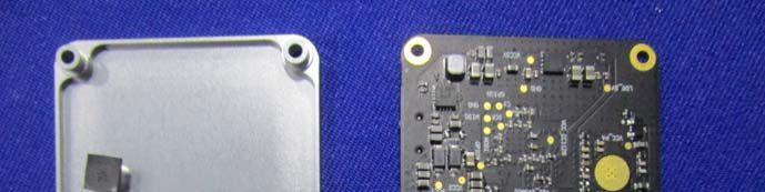
The primary PCB reveals a densely populated, high-quality assembly. The black soldermask and gold-plated contacts indicate a premium ENIG finish, while the presence of multiple surface-mount ICs points to a sophisticated blend of analog and digital processing. Prominently, a small microcontroller or RF transceiver is situated near the center, surrounded by supporting chips for power regulation and signal conditioning. Numerous vias—including via-in-pad and stitching—signal a multi-layer board optimized for high-speed and RF integrity. A metallic shield can covers the RF section, providing vital EMI/RFI suppression, while large capacitors and inductors ensure stable local power. The modular layout, with accessible test points and connectors, suggests a design built for both performance and serviceability. Overall, this section exemplifies best practices in RF module engineering, suitable for high-reliability wireless communication.

With the metal RF shield can removed, the underlying PCB section showcases several key ICs in both small-outline and larger QFN/BGA packages. The careful separation of analog/RF and digital domains is evident through distinct ground pours and strategic component placement. Multiple vias and decoupling capacitors surround the major ICs, underscoring a focus on signal and power integrity. The shield can itself demonstrates the module’s commitment to EMI/RFI mitigation, a necessity for any high-frequency wireless device. No antenna is visible here, but the density and arrangement of components strongly suggest this is the heart of the RF front-end, designed for minimal interference and maximum reliability.
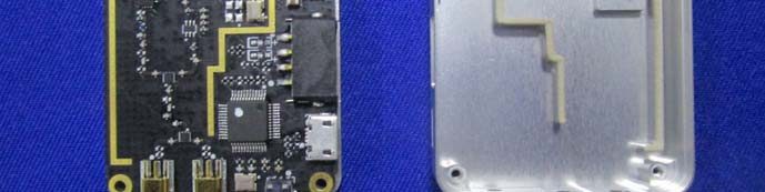
The juxtaposition of the left-side PCB and the right-side metallic enclosure highlights the dual priorities of signal integrity and physical robustness. At the PCB’s core sits a prominent QFP microcontroller or SoC, likely orchestrating both RF and digital functions. The controlled impedance traces and gold-plated edge contacts speak to meticulous RF engineering. Meanwhile, the metallic enclosure doubles as both an EMI shield and a possible integrated antenna structure, with trace geometries suggesting operation in the 2.4GHz or 5GHz bands. The inclusion of a micro-USB port and additional connectors points to flexible integration options, while the onboard power regulation ensures reliable, noise-free operation across all subsystems.
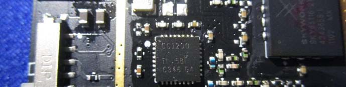
A close-up of the board reveals the Texas Instruments CC1200 RF transceiver at center stage—a highly regarded chip for sub-1 GHz narrowband communications. Its placement, surrounded by dense passives and carefully routed traces, illustrates the device’s focus on high-sensitivity RF performance and robust signal integrity. The gold trace near the board edge likely serves as the RF output path, leading to an external antenna connector. This section exemplifies precision RF layout, with abundant ground stitching and optimized impedance, ensuring the DATALINK PRO delivers both range and reliability in demanding telemetry applications.
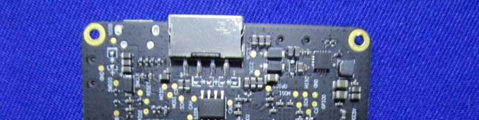
This PCB section reveals a sophisticated blend of power management, RF front-end, and signal conditioning. The presence of a shielded connector at the board’s edge suggests provision for a high-frequency external antenna or data interface. Multiple small-outline ICs, power inductors, and ceramic capacitors indicate robust local regulation and filtering—critical for minimizing noise in RF circuits. The use of ground pours, stitching vias, and a metallic shield can further underscores the device’s commitment to EMI/RFI control. The overall layout is compact, modular, and clearly engineered for integration into larger communication systems.
A focused view of the PCB’s RF or power management area reveals densely packed surface-mount components, including voltage regulators and logic ICs. The black soldermask, ENIG finish, and wide controlled-impedance traces reflect a design optimized for high-frequency signal integrity. The robust grounding strategy, with multiple stitching vias and copper pours, is evident throughout. The nearby metallic structure is likely a shielded connector or part of the RF shield, supporting both EMI suppression and mechanical stability. This section exemplifies the high-reliability design ethos necessary for professional-grade wireless modules.

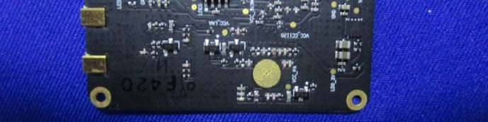
This close-up PCB segment showcases a dense array of passive components, small-outline ICs, and gold-plated edge pads. While no major SoCs or RF transceivers are visible here, the design’s sophistication is clear: multi-layer construction, precise SMD placement, and careful EMI-conscious layout. Gold-plated pads likely serve as board-to-board connectors or test points, while mounting holes with exposed copper rings provide mechanical support and possible grounding. The compactness and clean soldering reflect high manufacturing standards, underscoring the DATALINK PRO’s suitability for integration into mission-critical communication modules.
Regulatory Insights & FCC Filing
The FCC ID SS3-ZT300A1604 assigned to the DATALINK PRO by SZ DJI TECHNOLOGY is a definitive mark of compliance with US regulations governing radio frequency emissions and electromagnetic compatibility. This certification ensures the device meets all legal requirements for sale and deployment within the United States, safeguarding against harmful interference with other electronic equipment.
Although the grant date is listed as “None,” registration with the FCC (via FCC.gov) confirms the device has undergone rigorous evaluation. FCC filings typically encompass a wide range of technical documentation, including:
- Test Reports: Validating RF exposure, electromagnetic compatibility (EMC), and safety.
- Internal and External Photographs: Revealing construction and shielding methods.
- User Manuals and Operational Guides: Outlining safe and compliant usage.
- Block Diagrams and Schematics: Detailing internal circuitry and design.
- Label Placement and Compliance Statements: Demonstrating adherence to labeling requirements.
For integrators, engineers, and regulatory professionals, the presence of FCC ID SS3-ZT300A1604 assures that the DATALINK PRO is engineered and tested to prevent interference and operate safely within its specified frequency bands.
Potential Use Cases & Target Audience
The DATALINK PRO’s advanced wireless architecture and robust construction make it ideally suited for several demanding applications:
- Professional UAV & Drone Systems
-
Enables secure, long-range telemetry and real-time data links between airborne platforms and ground stations, supporting mission-critical operations such as surveying, inspection, and mapping.
-
Industrial Telemetry & Remote Monitoring
-
Provides reliable wireless communication for industrial automation, SCADA, and remote sensor networks, especially in environments where wired connectivity is impractical.
-
Research, Development, & System Integration
- Serves as a high-quality, modular RF link for engineers and developers building custom wireless solutions, test rigs, or field-deployable communication systems.
While the device does not specify a consumer target audience, its feature set and build quality clearly position it for professional, commercial, and industrial deployments where reliability, range, and regulatory compliance are non-negotiable.
Conclusion
The DATALINK PRO by SZ DJI TECHNOLOGY—certified under FCC ID SS3-ZT300A1604—embodies the pinnacle of wireless module engineering. Its sophisticated RF design, robust internal construction, and meticulous attention to EMI/RFI shielding ensure high reliability and performance in even the most challenging environments. The FCC certification not only legitimizes its use in the US market but also attests to its technical excellence and safety. For integrators and professionals seeking a dependable, high-performance wireless data link, the DATALINK PRO stands out as a compelling, standards-compliant choice in the world of advanced RF communications.