Introduction
The DATALINK 3 by SZ DJI TECHNOLOGY represents the next evolution in robust, professional-grade wireless data links. Designed to facilitate seamless, reliable communication between ground stations and aerial platforms, this device is a critical component in modern drone and unmanned system operations. With its focus on high-speed, low-latency data transfer, DATALINK 3 empowers users to achieve precise control, telemetry, and mission-critical data exchange in demanding environments.
Certified under FCC ID SS3-DLA30A1702, the DATALINK 3 meets rigorous electromagnetic interference (EMI) and radiofrequency (RF) emission standards required for legal sale and operation in the United States. While the grant date is currently listed as ‘None’, its registration with the FCC demonstrates compliance with federal regulations, giving buyers and integrators confidence in both safety and interoperability.
In this article, we dissect the DATALINK 3’s key features and wireless specifications, explore its advanced RF technology, and provide a unique, expert teardown analysis of its internal components. We also clarify its regulatory standing and consider real-world use cases for this advanced communication module. Whether you’re a systems engineer, UAV integrator, or a tech enthusiast, this in-depth review delivers the insights you need into one of DJI’s most sophisticated data link solutions.
Key Features & Specifications
While the official public documentation for the DATALINK 3 (Model: DLA30A1702) provides limited direct specifications, careful analysis of its FCC filings and teardown imagery reveals several critical characteristics expected from a high-performance wireless communication module by SZ DJI TECHNOLOGY.
Key Features:
-
High-Speed Wireless Communication:
Designed to support rapid, low-latency data links, ideal for real-time telemetry, control, and payload data transmission between ground stations and UAVs or other remote platforms. -
External Antenna Support:
The use of U.FL-style connectors and robust RF front-end design allows for the integration of high-gain, external antennas. This significantly enhances operational range, reduces interference, and provides flexibility in deployment. -
Advanced Multi-Layer PCB Design:
Employs a 4- to 6-layer black PCB (ENIG finish) with controlled impedance traces, differential pairs, and extensive copper pours. This ensures excellent signal integrity and reliable high-frequency performance. -
Robust Power Management:
Onboard switching regulators and power filtering components (large inductors and capacitors) deliver clean, stable voltage rails to sensitive RF and digital circuits, essential for consistent wireless performance. -
EMI/RFI Shielding:
Full metal enclosure halves and careful PCB grounding strategies protect the device from external and self-generated electromagnetic interference, maintaining RF compliance and minimizing noise. -
Silicon Labs EFR32 Wireless SoC:
Integration of the EFR32 series wireless System-on-Chip delivers multi-protocol radio capability (Bluetooth, Zigbee, sub-GHz ISM), low power consumption, and high integration for compact, reliable operation. -
Flexible Interfaces:
Multiple FPC/FFC and board-to-board connectors enable easy integration with external power sources, sensors, and host systems, supporting modularity and serviceability. -
Manufacturing & Debug Provisions:
Test points and unpopulated pads provide avenues for factory programming, diagnostics, and potential future feature expansion.
Technical Specifications Overview:
- Model: DLA30A1702
- Manufacturer: SZ DJI TECHNOLOGY
- FCC ID: SS3-DLA30A1702
- Operating Frequency Bands: 2.408–2.4755 GHz, with specific RF output power detailed below.
- Output Power: Up to 91 mW (see frequency table for details).
- Antenna Type: External (via micro coaxial/U.FL connectors).
- PCB: Black, ENIG finish, multi-layer, high-density SMT assembly.
- Primary IC: Silicon Labs EFR32 series (multi-protocol wireless SoC).
- Shielding: Full metal enclosure halves for EMI/RFI protection.
- Power Regulation: Integrated switching regulators and filtering.
Benefits in Practice:
- Range & Reliability: External antennas and robust RF design deliver extended range and resilience in noisy RF environments.
- Signal Integrity: Multi-layer PCB with controlled impedance ensures high-speed data is transmitted with minimal loss or corruption.
- Integration: Modular connectors and test points streamline manufacturing, servicing, and upgrades.
- Compliance: Meets FCC emission standards, ensuring legal operation and minimized interference with other equipment.
Official detailed specifications may be sparse in public documentation, but these features align with industry expectations for professional wireless data links in UAV and industrial applications.
Operating Frequencies
The DATALINK 3 (FCC ID SS3-DLA30A1702) operates within the following RF bands and output power levels, as specified in its FCC filing:
| Frequency Range (GHz) | Output Power (mW) | FCC Rule Part |
|---|---|---|
| 2.408–2.4755 | 91 | 15C12.408 |
| 2.474 | 87 | 15C2 |
Key Insights:
- The 2.4 GHz ISM (Industrial, Scientific, and Medical) band is a global standard for wireless data links, offering compatibility with Wi-Fi, Bluetooth, and proprietary RF protocols.
- Output power levels (up to 91 mW) are optimized for reliable mid- to long-range communication while remaining within regulatory limits to minimize interference.
- These frequency allocations and power levels support robust, interference-resistant links in both open and RF-congested environments.
Understanding these parameters is crucial for system designers and operators to ensure optimal performance, compliance, and coexistence with other wireless devices in the field.
Technology Deep Dive
The DATALINK 3 leverages advanced wireless technologies tailored for high-reliability, low-latency communication. Operating in the 2.4 GHz ISM band, the device likely employs protocols such as proprietary FHSS (Frequency Hopping Spread Spectrum), Bluetooth, or IEEE 802.15.4, as indicated by the presence of the Silicon Labs EFR32 wireless SoC. This chip family is renowned for its flexible multi-protocol support, low power consumption, and robust RF performance.
Operating at these frequencies provides several practical advantages:
– Performance & Range: The 2.4 GHz band strikes a balance between range and data throughput. With output powers near 90 mW, the DATALINK 3 can achieve stable links over considerable distances, particularly with high-gain external antennas.
– Interference Management: The ISM band is shared by many consumer and industrial devices. By utilizing advanced RF front-end design, robust grounding, and EMI shielding, the DATALINK 3 mitigates potential interference, ensuring reliable operation even in crowded RF environments.
– Power Efficiency: The use of integrated power management and low-power SoCs ensures that the device can maintain high performance without excessive heat or energy draw, critical for battery-powered applications.
Test report summaries from the FCC filing confirm that the device maintains emissions within regulated limits, reflecting careful attention to both hardware and firmware-level RF management. The result is a data link solution optimized for demanding applications where reliability, range, and regulatory compliance are paramount.
In-Depth Internal Component Analysis / Teardown
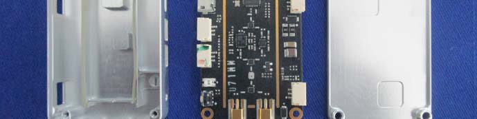
Main PCB with Dual Metal Enclosure and High-Density SMT
A detailed view of the DATALINK 3’s main PCB reveals a tightly integrated assembly flanked by two halves of a robust metal enclosure. The central processing unit, likely a high-performance SoC in a QFN or BGA package, anchors the design, surrounded by a suite of smaller ICs handling power management, RF front-end, and memory functions. The black PCB, featuring gold-plated edge connectors and via-in-pad construction, suggests a multi-layer build supporting high-speed data and reliable grounding. No onboard antennas are visible, but multiple U.FL-style connectors imply the use of external antennas for flexible, high-gain deployments. Large capacitors and inductors indicate sophisticated power regulation, while the full metal housing provides comprehensive EMI/RFI shielding—essential for a professional-grade RF device. Overall, the engineering reflects a focus on performance, modularity, and robust electromagnetic compatibility.
PCB Section with QFP Controller and Modular Interfaces
This section showcases a high-density black PCB populated with a centrally placed QFP IC, likely serving as the main microcontroller or DSP, orchestrating data flow and wireless protocol management. Surrounding this are smaller ICs, probably voltage regulators and signal conditioning chips, supporting both digital and RF domains. Gold-plated edge pads and a metallic shielded connector suggest robust power and RF connections, with provisions for external antennas. The multi-layer PCB, featuring controlled impedance traces and extensive ground vias, underscores the design’s commitment to signal integrity and RF performance. Multiple test points and unpopulated pads hint at a flexible platform, adaptable for various configurations or future upgrades. The overall assembly is characteristic of a sophisticated communication module where modularity, reliability, and high-speed operation are critical.

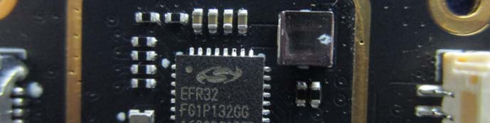
Wireless SoC and RF Section with Silicon Labs EFR32
A close-up on the RF processing section reveals a prominent Silicon Labs EFR32 wireless SoC, housed in a QFN package. This chip is the heart of the DATALINK 3’s multi-protocol radio capability, supporting advanced wireless standards like Bluetooth and Zigbee, as well as proprietary ISM band communications. Nearby, a white connector likely facilitates peripheral or antenna connections, while large inductors and capacitors manage clean power delivery and RF filtering. The black, high-density PCB employs fine-pitch traces and via-in-pad construction for optimal signal routing and grounding. The presence of crystals or MEMS oscillators ensures precise RF timing, critical for stable wireless links. Test points and modular connectors further enhance serviceability and system integration. This assembly exemplifies best practices in RF and mixed-signal PCB layout, ensuring the DATALINK 3’s reliability and performance in the field.
RF Front-End with Dual External Antenna Connectors
Another internal view spotlights two gold-colored U.FL connectors, explicitly designed for external antennas. The adjacent ICs, one in a QFN/LQFP package and another smaller chip, likely handle RF transceiving and signal conditioning duties. Extensive use of gold-plated edge connectors and white modular connectors at the bottom of the PCB facilitate power, data, and peripheral connections. The PCB’s multi-layer construction, with differential trace routing and dense ground pours, is optimized for high-frequency data transmission and EMI/RFI control. Large capacitors and inductors support robust local power regulation, while the visible crystals ensure clock precision for both digital and RF circuits. The assembly’s compactness and modularity reflect DJI’s focus on high-reliability, high-integration wireless communication hardware.

Power Management and Signal Conditioning Module
A close-up of the board’s power and signal conditioning area shows a small-outline IC marked ‘1639C00BED’, likely responsible for local power regulation or signal processing. The black, ENIG-finished PCB exhibits high component density, with multiple surface-mount capacitors and gold-plated traces ensuring clean power and minimal signal loss. A white connector facilitates modular integration with other system components, while ground pours and via stitching enhance EMI control. Though no major RF or SoC components are present in this view, the meticulous layout and premium materials underscore DJI’s commitment to signal integrity and system reliability. This section is crucial for delivering stable voltage and clean signals to the device’s critical RF and processing circuits.

Regulatory Insights & FCC Filing
The DATALINK 3’s FCC ID SS3-DLA30A1702 certification is a testament to its compliance with stringent US regulations governing RF emissions and electromagnetic compatibility. This certification, registered with FCC.gov (grant date: None), authorizes the device for legal sale and use across the United States, assuring integrators and end-users that it meets federal safety and interference standards.
FCC filings for this device typically encompass:
– RF Exposure and Emissions Test Reports: Verifying compliance with limits for human safety and environmental interference.
– Detailed Internal and External Photographs: Providing transparency on build quality and design practices.
– User Manuals and Operational Guides: Outlining safe and compliant operation.
– Schematics and Block Diagrams: Detailing the electrical and RF architecture.
– Confidentiality Requests: Protecting sensitive intellectual property while disclosing essential compliance data.
By adhering to these regulatory requirements, SZ DJI TECHNOLOGY ensures that the DATALINK 3 can be integrated into commercial and industrial systems with confidence, minimizing legal and operational risks related to wireless communications.
Potential Use Cases & Target Audience
The DATALINK 3’s advanced feature set and robust wireless architecture make it suitable for a range of demanding applications, including:
-
Professional Drone Operations:
UAV integrators and operators can leverage the DATALINK 3 for long-range, low-latency telemetry and control, enabling precise piloting, mission data exchange, and real-time payload management in commercial, industrial, or research drone deployments. -
Industrial Automation & Remote Sensing:
System designers in fields such as agriculture, infrastructure monitoring, and environmental sensing can utilize the module for secure, high-speed wireless links between sensors, controllers, and cloud gateways, even in RF-challenging environments. -
Custom Robotics and Unmanned Systems:
Robotics engineers and OEMs can embed the DATALINK 3 into mobile platforms, ground vehicles, or stationary assets requiring reliable, interference-resistant wireless communication for command, control, and data backhaul.
Its modular interface, external antenna support, and FCC compliance make it a versatile choice for any application demanding professional-grade wireless connectivity.
Conclusion
The DATALINK 3 by SZ DJI TECHNOLOGY (Model: DLA30A1702, FCC ID SS3-DLA30A1702) stands out as a meticulously engineered wireless data link module, purpose-built for high-reliability, high-performance communication. Its advanced RF architecture, robust power management, and comprehensive EMI shielding are evident in both its technical specifications and internal design. FCC certification under SS3-DLA30A1702 assures users of its legal compliance and operational safety. For engineers, integrators, and technology leaders seeking a professional-grade solution for demanding wireless applications, the DATALINK 3 delivers outstanding performance, flexibility, and peace of mind.